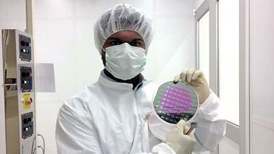
Masdar Institute's fabrication facility has now entered into the operational phase after researchers at the institute managed to "etch" a silicon wafer for the first time.
Etching is used to chemically remove layers from the surface of a silicon wafer during manufacturing.
This technique is used for chips in micro-electromechanical systems that can be found in smartphones, tablets, cameras and applications. The industry was worth US$1.9 billion (Dh6.97bn) last year.
Mike Tiner, the company's manager of fabrication and microscopy facilities, said: "Masdar Institute, Abu Dhabi and the UAE are well on their way to participating in an exciting technological revolution.
"This simple wafer, etched in a lab in Masdar Institute, represents the day that we made a significant step for the UAE to take its rightful place among those countries producing innovation for the world to share. The fabrication facility at Masdar Institute is a place for Emirati researchers, in their own country, that will encourage and support their contribution to this new and important scientific endeavour."
Ibrahim Elfadel, a professor of microsystems engineering, who is leading a multi-programme project on three-dimensional microelectronic circuit integration in collaboration with the Technical University of Dresden in Germany, said: "The hands-on learning will have direct bearing on several programmes at the institute, such as microsystems engineering, mechanical engineering, and materials science and engineering.
"It will also provide students and faculty involved in semiconductor research and manufacturing first-hand knowledge of the etching process. Masdar Institute's research projects which benefit from such first-hand knowledge include ongoing work on advanced semiconductor devices, 3D integration, and photonics."
* with additional reporting by Triska Hamid

